
First power is an experiment
PCB bring-up without guesswork
A new board has not earned trust yet. This sequence moves from documents to unpowered inspection, controlled first power, rails, code, interfaces, and load—one falsifiable observation at a time.
Written and verified by John Merton · verified 2026-07-11
The ordered workflow
Expected values are design-specific. The schematic, datasheets, tolerance analysis, and known-good evidence define them.
Know the board before touching power
Why: Catch revision and configuration mistakes before they become electrical symptoms.
- Put the schematic revision, PCB revision, BOM revision, assembly variant, and firmware build in the test record.
- Mark the expected input connector, voltage and polarity from the design—not from memory or a similar board.
- Draw the power tree: input protection, regulator inputs and outputs, enable signals, references, and the rails each load uses.
- Confirm pin 1, polarized parts, boot straps, reset network, programming header orientation, and the intended first-power state.
Stop condition: Stop if the physical board, BOM, schematic, or intended assembly variant do not agree. Resolve the source-of-truth mismatch first.
Unpowered inspection
Why: Find assembly defects and low-resistance paths without giving them energy.
- Inspect under magnification for bridges, solder balls, unsoldered pins, tombstones, shifted packages, damaged traces, debris, and connector damage.
- Verify every polarized or keyed part against the actual footprint and datasheet: diodes, electrolytics, IC pin 1, LEDs, batteries, and connectors.
- Measure resistance from each power rail to its return in both probe polarities. Compare with the design and a known-good board when one exists; charging capacitors and semiconductor junctions can make the reading move.
- Check that the input connector pinout and bench-lead polarity agree before attaching the supply.
Stop condition: Stop for an unexplained low-resistance rail, a polarity conflict, a bridge, or any assembly identity you cannot defend from the design files.
Bring-up / before power
Inspect the board you actually built.
The photograph shows real bench inspection. It does not prove power state, identify a fault, or stand in for your schematic and assembly record.
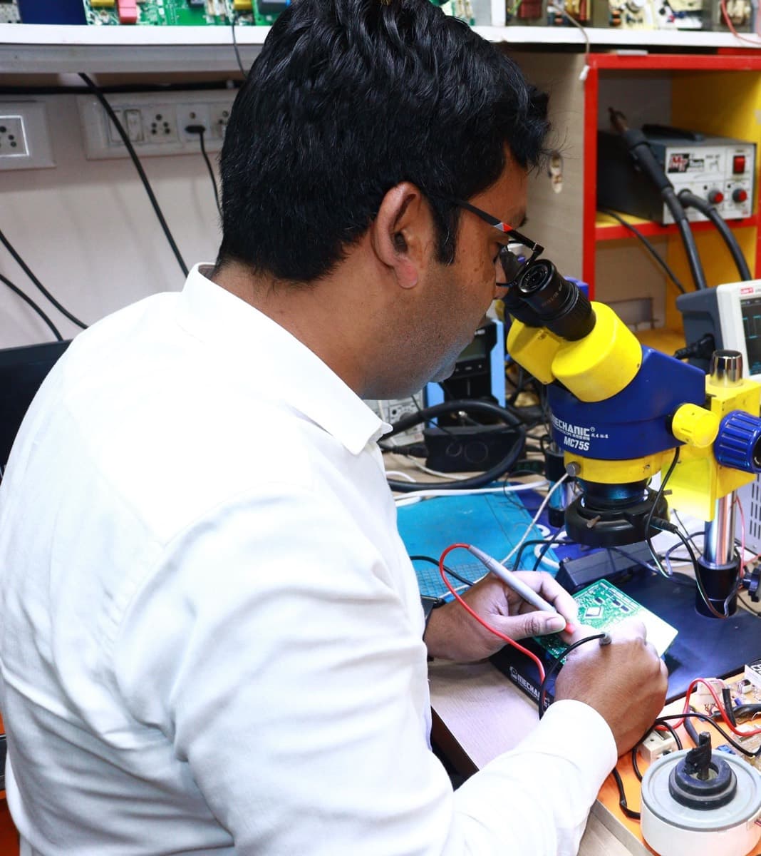
Documentary microscope context — no fault or power-state claim.
Photo: Multitech Institute / Pexels.Six jobs before power
Name the board and revision first.
Identity / revision
Confirm the physical assembly matches the intended build.
Connector polarity
Check entry points against the actual schematic and harness.
Pin 1 / polarized parts
Verify IC, diode, capacitor, and connector orientation.
Population / DNP
Compare fitted and omitted parts with the assembly record.
Solder / placement
Look for bridges, opens, tombstones, and mechanical damage.
Rail / test-point access
Plan safe measurement points before the board is energized.
Do not inferA clean-looking board is not evidence of correct rails, correct firmware, or safe first power.
Plan controlled first power
Why: Bound the energy available to a fault and decide what failure looks like before the board is live.
- Use the input voltage specified by the design. Do not invent a gentler voltage if regulators, supervisors, or startup circuits require a defined operating range.
- Choose an initial current limit from the board's expected startup and disabled-state loads. There is no universal safe number; document the design-specific basis.
- Disable or disconnect high-current loads and optional subsystems when the design permits independent startup.
- Place probes on the input and first critical rail before energizing so the first observation is deliberate rather than improvised.
Stop condition: Do not energize until the expected input, expected startup behavior, current-limit basis, probe reference, and stop conditions are written down.
Bring-up / controlled power
Power is a gated experiment.
The photo establishes real lab context. The diagram carries the procedure. They are intentionally not the same thing.
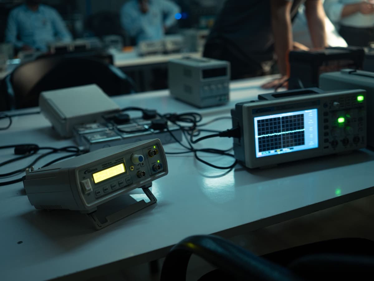
Documentary lab context — illustrative, not the depicted procedure.
Photo: khezez / Pexels.Source → DUT → observe
Copper = current path · green dash = observation
01 / Source
Bench supply
- Set voltage from design
- Use the board’s ground reference
- Set current limit from the budget
02 / DUT
Power entry
- Verify polarity before attach
- Check input and first critical rail
- Keep one shared reference node
03 / Observe
Measure, don’t assume
- Supply current display
- DMM rail measurement
- Optional thermal observation
Stop — remove powerUnexpected current · bad rail · unexpected heat · unstable supply
First power and immediate stop conditions
Why: Catch a destructive failure before troubleshooting turns into endurance testing.
- Energize while watching supply voltage and current. Distinguish normal startup charging from sustained current-limit operation using the design's expected behavior.
- Observe the input and first rail immediately, then check for unexpected heat with a suitable method that does not create a new short.
- If startup is clean, record input voltage, current draw, supply limit, and elapsed state before enabling more circuitry.
Stop condition: Remove power for unexpected current, a collapsed input, unexpected heat, smell, smoke, unstable supply behavior, or any rail outside the design-specific expected range. Do not repeatedly power-cycle an unexplained fault.
Bring-up / first power
First power is a gated experiment.
The photograph shows real instrument adjustment. It is not the depicted power-control procedure; the authored gate map carries that logic.
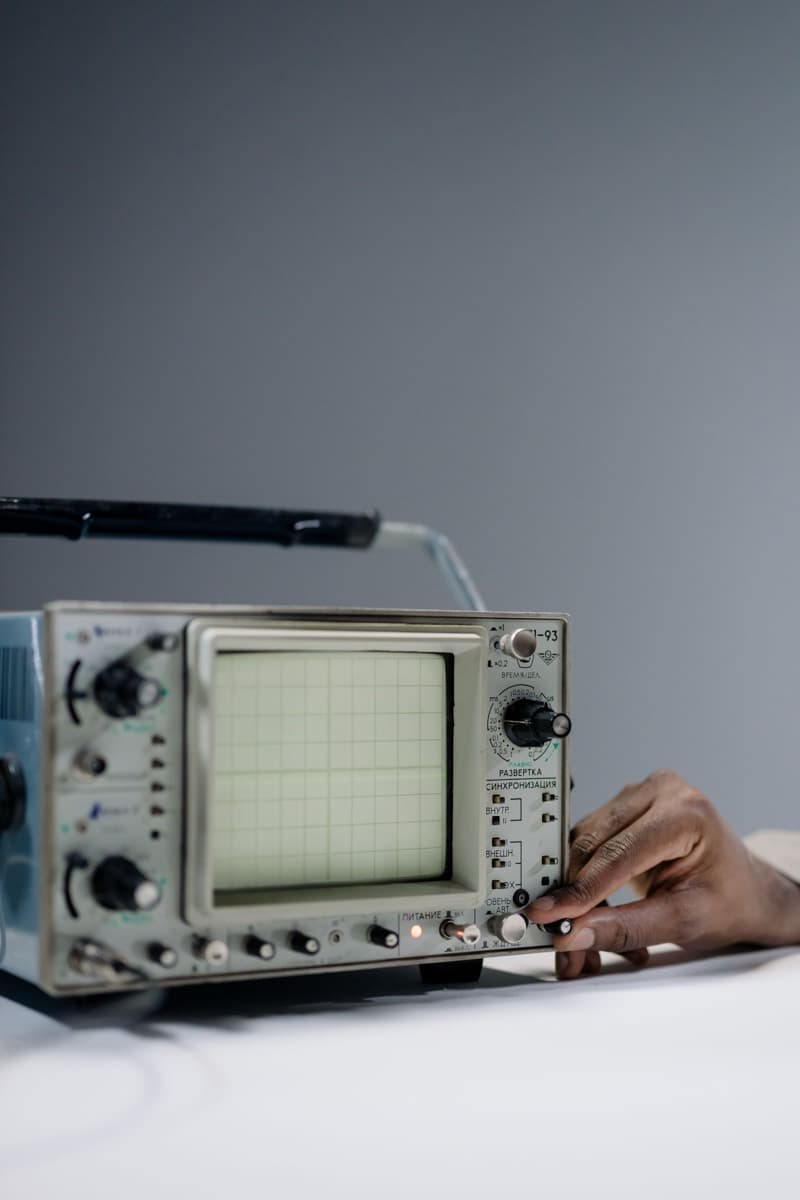
Real instrument adjustment — not the depicted first-power procedure.
Photo: cottonbro studio / Pexels.Advance only with evidence
Limits come from the actual design.
Unpowered inspection
Identity and polarity · rail-to-ground checks
Define the bounds
Set voltage from design · set current limit from the power budget
Configure the bench
Place probes first · write stop conditions before applying power
Apply power
Observe supply current · observe rail behavior
Earn the next step
Reset and clock · heat check before code
Stop — remove powerLimit hit · bad rail · unexplained heat · unstable reset or clock. Do not repeatedly power-cycle an unexplained fault.
Verify the power tree
Why: Localize a missing or wrong rail to the stage that creates or enables it.
- Walk the schematic in power-flow order: connector, protection element, regulator input, enable pin, regulator output, downstream switch, and load.
- Compare each rail and reference against the component datasheet and the design's tolerance budget, not a generic percentage.
- Check required sequencing and power-good relationships where the design depends on them.
- Use appropriate bandwidth and probing when checking ripple or regulator stability; a long ground lead can manufacture ringing that is not on the board.
Stop condition: Stop advancing when a rail, enable state, reference, or sequence is wrong. Diagnose that stage before connecting more loads or firmware complexity.
Clocks, reset, straps, and programming
Why: Separate power integrity from the minimum conditions required for code to execute.
- Confirm reset reaches the inactive state and that boot or mode straps match the intended startup path.
- Verify debugger or programmer reference voltage, ground, connector orientation, and signal continuity before blaming firmware.
- Check oscillator activity with a probe and point suitable for that circuit. Probe capacitance and ground inductance can stop or distort an oscillator.
- Load known-minimal firmware that proves one observable behavior before enabling the complete application.
Stop condition: If rails are correct but programming fails, hold application debugging. Resolve reset, straps, reference voltage, connector orientation, continuity, clocking, and device identity first.
Bring-up / observation geometry
Probe where the destination receives the signal.
The photograph shows generic meter contact. It is not an oscilloscope-grounding example. The authored panels carry the actual reset and clock rules.
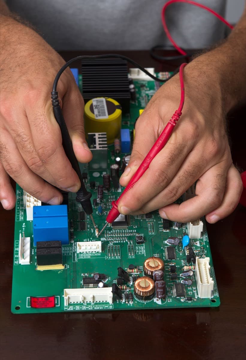
Generic meter-contact context — not the depicted scope method.
Photo: tnfeez design / Pexels.The observation includes the probe
Point · reference · bandwidth · scale · trigger
A · Reset
Destination pin or net
probe pointlocal reference- Active/inactive polarity comes from the design
- Capture around power-up
- No universal pulse-width claim
B · Clock
Destination clock
probe pointshort ground path- Observe frequency, amplitude, and edge
- Record bandwidth, scale, and trigger
- Use a differential method where required
Probe-loading warningA long ground lead can invent ringing. Crystal and high-impedance nodes may stop or distort when probed.
Validate interfaces incrementally
Why: Change one boundary at a time so a passing or failing observation has meaning.
- Start with the simplest available observability path, often a debugger or UART, before bringing up multiple buses at once.
- For I²C, SPI, UART, and GPIO, verify logic levels, pull-ups, addressing or chip select, pin mux, connector pinout, and a common reference.
- Bring up one peripheral at a time and record the transaction or physical observation that proves it works.
- If one peripheral fails, isolate it from the bus where possible and compare its power, reset, clock, and signal path with the schematic.
Stop condition: Do not change firmware, wiring, termination, and hardware simultaneously. Preserve one falsifiable next experiment.
Thermal and load checks
Why: Expose marginal power, assembly, and thermal behavior after idle bring-up passes.
- Record idle current and look for unexpected hot spots before applying load.
- Increase load or enable subsystems in controlled steps while re-checking input current, critical rails, regulator behavior, and component temperature against design limits.
- Exercise intended operating modes, connectors, and duty cycles without exceeding the validated bench setup.
- Re-check rails after the board warms; a board that passes only cold has not passed bring-up.
Stop condition: Remove power for unexpected temperature rise, rail collapse, oscillation, current-limit entry, or intermittent behavior. Return to the last known-good load step.
Record the known-good baseline
Why: Turn one successful board into evidence that can diagnose the next board.
- Record board and assembly revision, firmware revision, supply model and settings, probe setup, ambient conditions, and connected loads.
- Capture rail measurements, idle and active current, reset and clock observations, interface checks, and thermal observations.
- Save clear photos of setup and probe points, along with failures encountered and the experiment that resolved each one.
- Name the remaining untested risks. A functioning demo is not proof that every operating corner is validated.
Stop condition: Do not call the baseline reproducible until another person can identify the board, setup, expected values, and pass/fail evidence from the record.
Failure decision tree
Start at the first failed boundary. Later symptoms are often downstream noise.
- Current limit is reached immediately
- Power off. Recheck rail resistance, polarity, bridges, reversed parts, input protection, and isolated power domains.
- Input is present but a rail is missing
- Trace input → protection → regulator input → enable → output → load. The first wrong node bounds the fault.
- Rails are correct but programming fails
- Verify target identity, reset, straps, reference voltage, connector orientation, continuity, clock assumptions, and programmer settings.
- Firmware runs but one peripheral fails
- Check that peripheral's power/reset/clock, pin mux, logic levels, address or chip select, pull-ups, connector path, and minimal transaction.
- The board works intermittently or only when probed
- Suspect marginal joints, floating inputs, reset timing, probe loading, inadequate decoupling, return-path problems, or thermal sensitivity. Record exactly what the probe changes.
Tools used in this workflow
You do not need every tool at once. Choose equipment for the measurement job and its voltage, energy, bandwidth, and isolation requirements. The source-backed PCB bench guide covers a restrained low-voltage starter setup.
Explore the whole system
A bench measurement makes more sense when you can trace it through the complete circuit job.
- PCB Bring-Up and Debugging SystemMove from unpowered inspection through controlled first power, rails, clocks, reset, programming, interfaces, load, and a reproducible baseline.
- PCB Power-Tree DesignDesign a PCB power tree from input protection through conversion, regulation, sequencing, measurement, and load verification.
- USB Interface Design for PCBsConnect USB power, the physical receptacle, ESD strategy, data routing, and a bridge or native-USB controller without guessing at pinouts.
- Sensor-Node PCB DesignDesign a sensor node around power integrity, interface constraints, address conflicts, placement, calibration, and observable failure modes.
- Motor-Control PCB DesignChoose and bring up a motor driver using real current, supply, decay, protection, thermal, and layout constraints.
Common questions
What should I do before applying power to a new PCB for the first time?
Know the board first: record schematic, PCB, BOM, and firmware revisions, confirm the expected input connector, voltage, and polarity from the design, and draw the power tree. Then do an unpowered inspection—check for bridges, solder balls, damaged traces, and measure resistance from each rail to its return before energizing anything.
What is a safe way to apply first power to a new board?
Use the input voltage the design specifies, choose an initial current limit from the board's expected startup and disabled-state loads, and disable high-current or optional subsystems when the design allows independent startup. Place probes on the input and first critical rail before energizing so the first observation is deliberate.
When should I stop and remove power during PCB bring-up?
Remove power immediately for unexpected current, a collapsed input, unexpected heat, smell, smoke, unstable supply behavior, or any rail outside the design's expected range. Do not repeatedly power-cycle an unexplained fault—resolve the source of the fault before reapplying power to the board.
What should I check if a rail is missing but the input is present?
Trace the schematic in power-flow order: connector, protection element, regulator input, enable pin, regulator output, downstream switch, and load. The first wrong node in that chain bounds the fault—compare each rail and reference against the component datasheet and the design's own tolerance budget, not a generic percentage.
Method, sources, and corrections
This checklist synthesizes manufacturer bring-up guidance and instrument-vendor probing guidance. It deliberately omits universal current limits, rail tolerances, temperatures, and probe ratings because those belong to the actual design and instrument manuals. Source scope and caveats are recorded in the project research manifest. Corrections are welcome at corrections@pcbwiki.com.
Found an error? Submit a correction — we verify every correction against the manufacturer’s datasheet.